- 您现在的位置:买卖IC网 > Sheet目录3832 > AT87C52X2-3CSUM (Atmel)IC 8051 MCU 8K OTP 40MHZ 40DIP
38
TS8xCx2X2
4184I–8051–02/08
DC Parameters for Low
Voltage
TA = 0°C to +70°C; VSS = 0 V; VCC = 2.7 V to 5.5V ; F = 0 to 30 MHz.
TA = -40°C to +85°C; VSS = 0 V; VCC = 2.7 V to 5.5V ; F = 0 to 30 MHz.
Notes: 1. ICC under reset is measured with all output pins disconnected; XTAL1 driven with TCLCH, TCHCL = 5 ns (see Figure 17.), VIL =
VSS + 0.5V,
VIH = VCC - 0.5V; XTAL2 N.C.; EA = RST = Port 0 = VCC. ICC would be slightly higher if a crystal oscillator used..
2. Idle ICC is measured with all output pins disconnected; XTAL1 driven with TCLCH, TCHCL = 5 ns, VIL = VSS + 0.5V, VIH = VCC -
3. Power Down ICC is measured with all output pins disconnected; EA = VSS, PORT 0 = VCC; XTAL2 NC.; RST = VSS (see Fig-
4. Capacitance loading on Ports 0 and 2 may cause spurious noise pulses to be superimposed on the VOLs of ALE and Ports 1
and 3. The noise is due to external bus capacitance discharging into the Port 0 and Port 2 pins when these pins make 1 to 0
transitions during bus operation. In the worst cases (capacitive loading 100pF), the noise pulse on the ALE line may exceed
0.45V with maxi VOL peak 0.6V. A Schmitt Trigger use is not necessary.
5. Typicals are based on a limited number of samples and are not guaranteed. The values listed are at room temperature and
5V.
6. Under steady state (non-transient) conditions, IOL must be externally limited as follows:
Maximum IOL per port pin: 10 mA
Maximum IOL per 8-bit port:
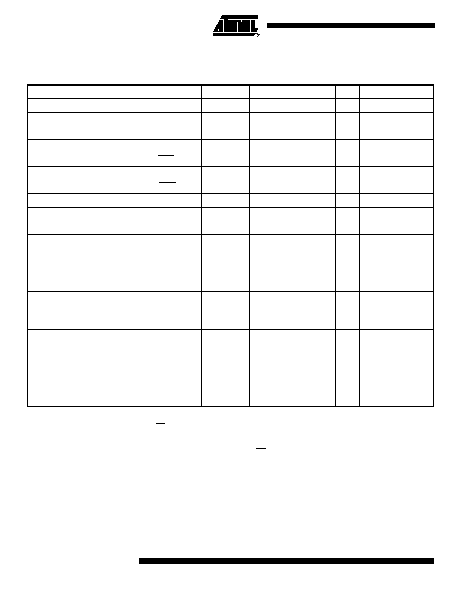
Table 23. DC Parameters for Low Voltage
Symbol
Parameter
Min
Typ
Max
Unit
Test Conditions
VIL
Input Low Voltage
-0.5
0.2 VCC - 0.1
V
VIH
Input High Voltage except XTAL1, RST
0.2 VCC + 0.9
VCC + 0.5
V
VIH1
Input High Voltage, XTAL1, RST
0.7 VCC
VCC + 0.5
V
VOL
Output Low Voltage, ports 1, 2, 3 (6)
0.45
V
IOL = 0.8 mA(4)
VOL1
Output Low Voltage, port 0, ALE, PSEN (6)
0.45
V
IOL = 1.6 mA(4)
VOH
Output High Voltage, ports 1, 2, 3
0.9 VCC
V
IOH = -10 A
VOH1
Output High Voltage, port 0, ALE, PSEN
0.9 VCC
V
IOH = -40 A
IIL
Logical 0 Input Current ports 1, 2 and 3
-50
A
Vin = 0.45V
ILI
Input Leakage Current
±10
A
0.45V < Vin < VCC
ITL
Logical 1 to 0 Transition Current, ports 1, 2, 3
-650
A
Vin = 2.0 V
RRST
RST Pulldown Resistor
50
90 (5)
200
k
CIO
Capacitance of I/O Buffer
10
pF
Fc = 1 MHz
TA = 25°C
IPD
Power Down Current
20 (5)
10 (5)
50
30
A
VCC = 2.0 V to 5.5V(3)
VCC = 2.0 V to 3.3 V(3)
ICC
under
RESET
Power Supply Current Maximum values, X1
mode: (7)
1 + 0.2 Freq
(MHz)
at12MHz 3.4
at16MHz 4.2
mA
VCC = 3.3 V(1)
ICC
operating
Power Supply Current Maximum values, X1
mode: (7)
1 + 0.3 Freq
(MHz)
at12MHz 4.6
at16MHz 5.8
mA
VCC = 3.3 V(8)
ICC
idle
Power Supply Current Maximum values, X1
mode: (7)
0.15 Freq
(MHz) + 0.2
at12MHz 2
at16MHz 2.6
mA
VCC = 3.3 V(2)
发布紧急采购,3分钟左右您将得到回复。
相关PDF资料
PIC16C924-04/L
IC MCU OTP 4KX14 LCD DVR 68PLCC
PIC16F767-I/SO
IC PIC MCU FLASH 8KX14 28SOIC
PIC24FJ64GA310-I/PF
MCU 16BIT 64KB FLASH 100TQFP
DSPIC33FJ64GP202-E/MM
IC DSPIC MCU/DSP 64K 28-QFN
PIC16F876A-I/ML
IC MCU FLASH 8KX14 A/D 28QFN
PIC16F876A-I/SO
IC MCU FLASH 8KX14 EE 28SOIC
PIC16F876A-I/SP
IC MCU FLASH 8KX14 EE 28DIP
AT87C51RD2-3CSUM
IC 8051 MCU 64K OTP 40MHZ 40DIP
相关代理商/技术参数
AT87C52X2-3CSUV
功能描述:8位微控制器 -MCU Microcontroller
RoHS:否 制造商:Silicon Labs 核心:8051 处理器系列:C8051F39x 数据总线宽度:8 bit 最大时钟频率:50 MHz 程序存储器大小:16 KB 数据 RAM 大小:1 KB 片上 ADC:Yes 工作电源电压:1.8 V to 3.6 V 工作温度范围:- 40 C to + 105 C 封装 / 箱体:QFN-20 安装风格:SMD/SMT
AT87C52X2-RLRUM
功能描述:8位微控制器 -MCU 0.5um RoHS:否 制造商:Silicon Labs 核心:8051 处理器系列:C8051F39x 数据总线宽度:8 bit 最大时钟频率:50 MHz 程序存储器大小:16 KB 数据 RAM 大小:1 KB 片上 ADC:Yes 工作电源电压:1.8 V to 3.6 V 工作温度范围:- 40 C to + 105 C 封装 / 箱体:QFN-20 安装风格:SMD/SMT
AT87C52X2-RLTUL
功能描述:8位微控制器 -MCU C72X2C52 0.5m OTP RoHS:否 制造商:Silicon Labs 核心:8051 处理器系列:C8051F39x 数据总线宽度:8 bit 最大时钟频率:50 MHz 程序存储器大小:16 KB 数据 RAM 大小:1 KB 片上 ADC:Yes 工作电源电压:1.8 V to 3.6 V 工作温度范围:- 40 C to + 105 C 封装 / 箱体:QFN-20 安装风格:SMD/SMT
AT87C52X2-RLTUM
功能描述:8位微控制器 -MCU C72X2 C52 0.5 m X 2 OTP 0.5 NV RoHS:否 制造商:Silicon Labs 核心:8051 处理器系列:C8051F39x 数据总线宽度:8 bit 最大时钟频率:50 MHz 程序存储器大小:16 KB 数据 RAM 大小:1 KB 片上 ADC:Yes 工作电源电压:1.8 V to 3.6 V 工作温度范围:- 40 C to + 105 C 封装 / 箱体:QFN-20 安装风格:SMD/SMT
AT87C52X2-RLTUV
制造商:ATMEL 制造商全称:ATMEL Corporation 功能描述:8-bit Microcontroller 8 Kbytes ROM/OTP, ROMless
AT87C52X2-SLRUL
功能描述:8位微控制器 -MCU Microcontroller RoHS:否 制造商:Silicon Labs 核心:8051 处理器系列:C8051F39x 数据总线宽度:8 bit 最大时钟频率:50 MHz 程序存储器大小:16 KB 数据 RAM 大小:1 KB 片上 ADC:Yes 工作电源电压:1.8 V to 3.6 V 工作温度范围:- 40 C to + 105 C 封装 / 箱体:QFN-20 安装风格:SMD/SMT
AT87C52X2-SLRUM
功能描述:8位微控制器 -MCU Microcontroller RoHS:否 制造商:Silicon Labs 核心:8051 处理器系列:C8051F39x 数据总线宽度:8 bit 最大时钟频率:50 MHz 程序存储器大小:16 KB 数据 RAM 大小:1 KB 片上 ADC:Yes 工作电源电压:1.8 V to 3.6 V 工作温度范围:- 40 C to + 105 C 封装 / 箱体:QFN-20 安装风格:SMD/SMT
AT87C52X2-SLSUL
功能描述:8位微控制器 -MCU OTP C52/8K 40MHZ 3V COM RoHS:否 制造商:Silicon Labs 核心:8051 处理器系列:C8051F39x 数据总线宽度:8 bit 最大时钟频率:50 MHz 程序存储器大小:16 KB 数据 RAM 大小:1 KB 片上 ADC:Yes 工作电源电压:1.8 V to 3.6 V 工作温度范围:- 40 C to + 105 C 封装 / 箱体:QFN-20 安装风格:SMD/SMT